
Parasitic Impedance and Signal Reflection
In RF (Radio Frequency) circuit design on PCB, ensuring good signal transmission at high frequencies requires engineers not only to understand basic electrical circuit principles but also to have a solid knowledge of electromagnetic wave behavior and signal characteristics on transmission lines. At high-frequency ranges, where signals should be treated as electromagnetic waves moving through conducting structures, factors such as characteristic impedance, parasitic impedance, and signal reflection become important elements that affect signal integrity and the overall system performance.
This sharing focuses on presenting the fundamental concepts in RF circuit design, including: complex impedance and its role in the frequency domain; common types of parasitic impedance found on PCBs; the causes and effects of signal reflection due to impedance mismatch; and the reflection coefficient, which describes the level of reflection on a transmission line. Understanding and controlling these factors is an essential first step to optimizing RF design on PCBs, improving signal transmission efficiency, and reducing loss in modern RF applications.
Section 1: Parasitic Impedance
1.1. Overview of Impedance
In an ideal DC circuit, a component can be described only by its resistance. However, in reality, a DC circuit may have changing signals, or it may be an AC circuit, where impedance exists. Impedance is a measure of how much the circuit resists the flow of electric current, and it includes resistance, inductive reactance, and capacitive reactance. Basically, it is the ratio of voltage to current, expressed in the frequency domain. Impedance is a complex number, which includes a real part and an imaginary part.
Where:
- is the complex impedance
- is the resistance (the real part)
- is the reactance (the imaginary part), which includes both capacitive and inductive reactance
Resistance is always positive, while reactance can be either positive or negative. Resistance in a circuit dissipates energy as heat, while reactance stores energy — capacitive reactance stores energy in the form of an electric field, and inductive reactance stores energy in the form of a magnetic field.
1.2. Parasitic Impedance
Parasitic impedance is an unwanted impedance that includes capacitance, inductance, and resistance arising in electronic circuits, especially in PCB designs. This impedance is not intentionally designed but naturally occurs due to the physical properties of materials, circuit traces, and components during design and manufacturing.
At high frequencies, parasitic impedance becomes an important factor affecting system performance. Parasitic elements in the PCB, components, and connections can cause signal loss, unwanted reflections, crosstalk, and significantly reduce the overall performance of RF circuits.
The components that cause parasitic impedance include:
- Parasitic Resistance: Parasitic resistance causes power loss in RF transmission lines. It appears in PCB traces, conductors, and passive components.
- Parasitic Capacitance: Parasitic capacitance leads to crosstalk and signal reflection. It occurs when PCB traces are close to each other or within electronic components.
- Parasitic Inductance: Parasitic inductance causes interference and signal degradation at high frequencies. It occurs in vias, connection points, wiring, or electronic components.
Section 2: Signal Reflection
2.1. Overview of Reflection
2.1.1. Reflection phenomenon
Reflection, refraction, diffraction, and interference — all classical wave phenomena — apply to electromagnetic radiation. However, within the scope of this article, we focus only on electrical signals in circuits that have not yet been converted into electromagnetic radiation by an antenna. Therefore, we will only discuss the reflection and interference of signals.
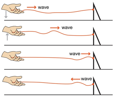
Reflection occurs when a wave encounters an obstacle that does not fully absorb the wave, or absorbs part of its energy, while the rest is reflected back. Similarly, in electromagnetic radiation, the obstacle refers to electronic components on the circuit, with impedance being the parameter that causes reflection — a measure of how much the circuit resists the electric current.
In reality, electrical signals do not travel only one way from the source to the load; there is also a reflected signal traveling back. In other words, on a signal path, signals exist in both directions: from the source to the load, and the reflected signal from the load back to the source.
This phenomenon causes adverse effects because reflected waves can lead to signal loss, distortion, and interference. This is especially critical when designing high-frequency signal circuits such as RF circuits, resulting in energy loss, electromagnetic interference, and a significant reduction in circuit performance.
2.1.2. Handling signal reflection
To handle signal reflection, it is necessary to minimize the amount of signal that can be reflected back. Impedance, which measures the resistance to electric current, is the main factor causing signal reflection. To reduce reflection, the effect of impedance mismatch must be minimized. With proper impedance matching, there is no interruption, and the load can absorb all the signal energy.
According to the Maximum Power Transfer Theorem (which will be discussed in a future article), maximum power is achieved when the magnitude of the load impedance equals the magnitude of the source impedance (including the characteristic impedance of the transmission line).
The amount of reflected energy depends on the severity of the impedance mismatch. The two worst cases are open circuit (infinite impedance) and short circuit (zero impedance). In both cases, all the energy is reflected back.
2.2. Reflection Coefficient
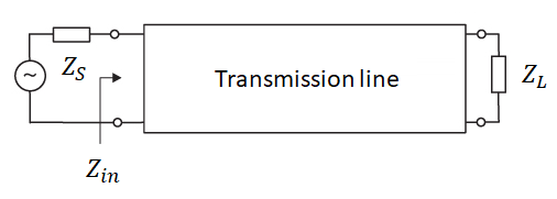
The reflection coefficient represents the amount of wave reflected back when passing through an interface with impedance mismatch.
2.2.1. Reflection Coefficient at the Load
Where:
- is the load impedance
- is the characteristic impedance of the transmission line
- is the reflection coefficient, which ranges , the larger the value, the higher the reflection coefficient
2.2.2. Reflection Coefficient at the Source
Reflection at the source occurs when the signal is reflected back toward the input of the transmission line:
Where:
- is the input impedance of the transmission line
- is the source impedance
- is the reflection coefficient, which ranges , the larger the value, the higher the reflection coefficient
2.3. The problems of Signal Reflection
Consider a simple circuit consisting of a sine wave source operating at a frequency of 2.4 GHz, a transmission line with a length of one-quarter wavelength, and the circuit is fully impedance-matched at 50 Ohms (including the impedance at the source, load, and transmission line). The green measurement point represents the wave at the source, and the red measurement point shows the wave at the load (the wave after traveling through the transmission line).
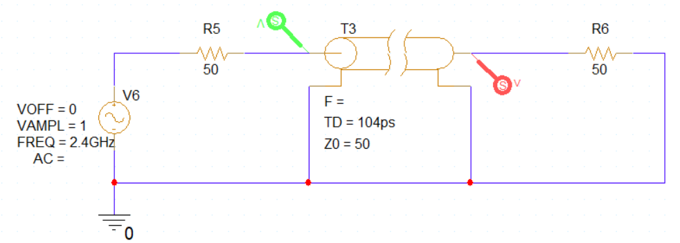
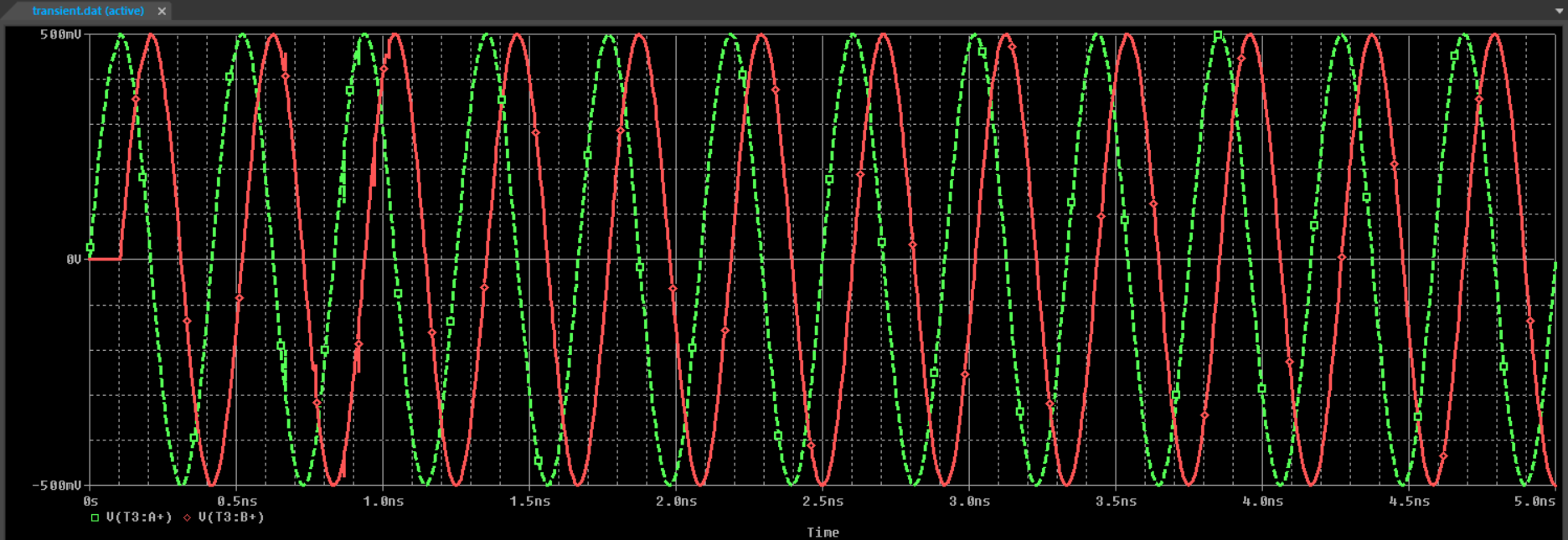
Since the circuit is fully impedance-matched, there will be no reflected wave. The wave measured at the red point is phase-delayed by exactly one-quarter wavelength compared to the wave at the green point, with both having the same amplitude at 500 mV.
To examine the adverse effects of an impedance mismatch in a circuit, we can perform simulations and some calculations as follows:
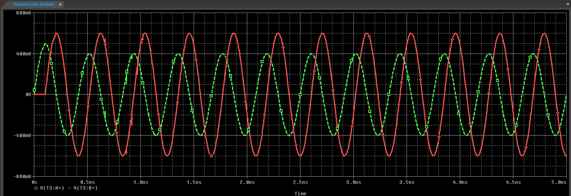
Consider a circuit with an impedance mismatch at the load, where the load impedance is 75 ohms. Note that at the wave at the load (the end of the transmission line), when the wave is just transmitted from the source and traveling along the line (before any reflection occurs at the load), the current wave amplitude is 500 mV. However, after traveling one-quarter wavelength, reflection occurs at this moment.
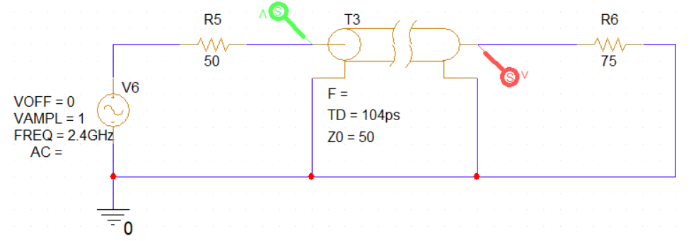
If there were no reflection as in the first case (perfect impedance matching), the wave amplitude would remain unchanged. But in this case, the incident wave interferes with the reflected wave, causing the amplitude at the load to increase to 600 mV and the amplitude at the source to decrease to 400 mV after the reflected wave travels back toward the source.
We can perform some calculations as follows:
First, we can calculate the reflection coefficient at the load.
means that 20% of the wave energy has been reflected back into the transmission line.
We consider the wave equation with a wave propagation distance
Taking the reference point at the source, the wave at the source has the wave equation traveling along the transmission line as , the wave at the end of the transmission line (ignoring any reflected wave) is delayed by one-quarter wavelength:
The reflected wave at the load with reflection coefficient is:
Here, we can calculate the interference wave at the load, which is the interference between the wave at the end of the transmission line and the reflected wave at the load with reflection coefficient :
The reflected wave traveling back to the source will cover a distance of , moving in the opposite direction to the incident wave. We can calculate the interference wave at the source as follows:
By substituting the wave amplitudes and the reflection coefficient values, we can calculate the interference wave amplitudes at the source and load as 400 mV and 600 mV, respectively.
This shows the adverse effects of impedance mismatch, where wave reflection can alter the wave characteristics due to interference. The simplest impact is the change in wave amplitude, which means the voltage on the transmission line varies. This can cause the signal to be too weak or, in worse cases, damage the circuit if components cannot withstand the increased voltage.
However, the problem above only considers the wave equation in the time domain at two points: the source and the load. In reality, the interference wave traveling along the transmission line behaves more complexly.
Refer to the article Reflections from Impedance and the Standing Wave Ratio for a visual observation of the interference wave behavior.
The interference wave’s amplitude changes continuously, and at each point along the transmission line, the wave may not follow a single wave equation. Looking back at the problem above, the wave equations at the source and load are different. This can lead to uncontrolled effects, causing interference not only on the transmission line but also radiating outward, which is difficult to control.
The problem above only considers impedance mismatch at the load. In reality, if not well controlled, impedance mismatch can occur at the source and along the transmission line itself. Waves may reflect multiple times on the line, reflecting continuously, leading to extreme behaviors in the circuit.
Observe the behavior of the sample reflected wave in Desmos using the mathematical model we have constructed.
References
Brian C. Wadell. Transmission Line Design Handbook. Artech House, Boston, 1991.
Infineon Technologies. Antenna Design and RF Layout Guidelines, 2023.
Cadence Blog. How to Use a Transmission Line Reflection Coefficient Correctly, 2021.
Cadence Blog. The Fundamental Frequency and Harmonics in Electronics. 2023.
Cadence Blog. S-Parameters and the Reflection Coefficient. 2023.
Cadence System Analysis. How signal reflection and impedance mismatch are related, 2021.
Cadence Design Systems. Conjugate matching vs. reflectionless matching in electronic circuits, 2021.
All About Circuits. Introduction to impedance matching using transmission line elements, 2023.
All About Circuits. Understanding reflections and standing waves in RF circuit design, 2023.